posted in Technology

Chinese CXMT to Match Micron's DRAM Manufacturing Capacity This Year

A particularly surprising discovery is that CXMT is constructing its cleanrooms—where the actual silicon is produced—in just around 12 months, whereas the rest of the DRAM manufacturing industry typically takes 21-24 months, nearly a full year longer.

Finally, the report notes that the Chinese government is encouraging CXMT to transfer its DRAM technology IP to other Chinese DRAM manufacturers such as JHICC, Swaysure, and YTMC’s subsidiary XMC. This initiative aims to alleviate memory shortages domestically before CAMT-designed DRAM enters other markets, such as the EU and possibly even the U.S.
www.techpowerup.com/350726/chinese-cxmt-to-match-microns-dram-manufacturing-capacity-this-year
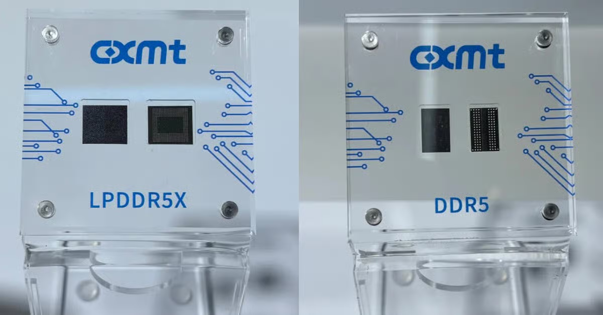
TechPowerUpChinese CXMT to Match Micron's DRAM Manufacturing Capacity This YearChinese memory giant CXMT has been expanding its capacity so rapidly that the company is now able to compete with one of the largest memory manufacturers in the world—Micron. According to analysis from Citrini Research and their proprietary data, CXMT is projected to produce about 350,000 DRAM...


Replying to an earlier post

It hasn’t felt t like there’s been much significant performance increases or development in RAM in the last.. decade? Definitely not following moores law (if that even applies here). So if youve spent your time price fixing for the western market instead of developing technology to keep you ahead, then second rate competitors will eventually catch up and cut a huge portion of your market share, and enjoy those inflated prices instead of you. This of course is my very uninformed take, and probably completely inaccurate.

Replying to @⁨ToiletFlushShowerScream@piefed.world⁩

It hasn’t felt t like there’s been much significant performance increases or development in RAM in the last… decade?

In memory? There’s been a ton of improvement, even if most of the coolest stuff isn’t making it into DIMMs that are installed in user laptops/desktops.

Advanced packaging technology has allowed chip manufacturers to put different silicon dies together with increasingly high performance (high bandwidth, low latency) connections in the same package, including with some three dimensional stacking. That way they can mix and match different silicon dies for greater cost effectiveness, yield, performance, etc.

This also means that in-package memory is now the standard in certain chips. Apple’s M-series silicon has its memory packaged right into the CPU/GPU package, as a system-in-a-package, so that the connection between the logic and memory is comparatively much higher performance, several times higher bandwidth than desktops or laptops that don’t follow that kind of architecture.

Similarly, in data centers, the AI boom has caused all the memory manufacturers to switch their production lines to high bandwidth memory, where they vertically stack a bunch of DRAM chips on each other, with ultra-fast, high bandwidth connections, so that they can shove terabytes of memory into these data center servers. These recent generations have been improving speed and bandwidth in ways that make consumer level DDR5 RAM look like child’s play.

So they’re improving things. Just not in ways that really show up in DIMM sticks.

newsletter.semianalysis.comScaling the Memory Wall: The Rise and Roadmap of HBMHBM4, Custom Base Die, Shoreline Expansion, Process Flow, China Domestic Production, Samsung Qualification